Zainalabedin Navabi and Armita Peymandoust
Electrical and Computer Engineering Department
Northeastern University
Boston, Massachusetts 02115
navabi@ece.neu.edu
Event driven simulation speed can be improved by reducing events that cause unnecessary simulation activities. Events due to data scheduling account for a large portion of simulation time. We have developed RTL component modeling strategies with explicit scheduling and reduced activity. This paper discusses activity suppression techniques and their implementation in VHDL.
Activity reduction and cycle based simulation techniques suggest new ways of modeling components in VHDL. By studying these methods and experimenting with various modeling styles in VHDL, we have developed a style for modeling RTL components that simulate at least twice as fast as standard RTL descriptions that are developed for synthesis. In this new modeling style, signals are removed and replaced with shared variables. Such replacement requires the flow of data in an RTL description to be explicitly controlled by control signals.
The main concept behind the suggested modeling style is the reduction of activities [4]. This is done for the registers, buses, logic units, and controller of a system. Our suggested modeling style focuses on reducing activities by
-
1) Prioritizing register control lines,
2) Toggling control signals,
3) Removal of Z values,
4) Reducing interconnection line activities, and
5) Using explicit timing. Each of these issues will be discussed in the following paragraphs.
The implementation of the topics discussed in the pervious section requires the use of Shared Variables and other VHDL'93 constructs. Figures 1 and 2 are illustration of changes that are done to a synthesizable RTL model for reduction of activities. Figure 1 shows activities in an RTL description that can be eliminated for faster simulation. Figure 2 shows an outline and the bussing structure of a reduced-activity description. In this section we will discuss the VHDL coding style for the implementation of these changes. We will discuss shared variable busses, logic sensitivities, register control signals, and control signal timing.
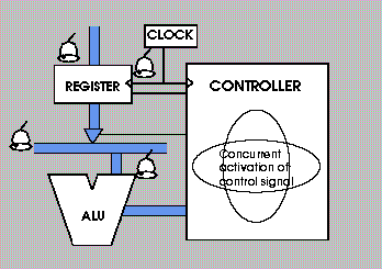
Figure 1. Signal activities in RTL synthesizable descriptions
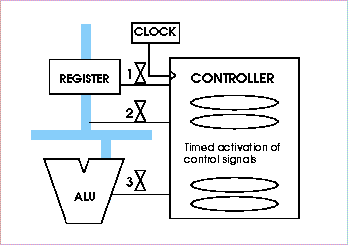
Figure 2. Activities are reduced to those on timed control signals
In our style of description, all buses and interconnection lines are replaced by shared variables. Changing the value of signals causes events or activities, yet assigning new values to variables does not result in events. Therefore, this greatly reduces activities while data is being moved from one register to another and perhaps even through logic units. Input or output of a register connected to a bus uses the same name as the bus. This way, the register model will not have any internal assignments to its ports.
This section describes transformation of synthesizable models into modified RTL models for faster simulation. The synthesizable model RTL used as a starting point is described in section 3.1. The details of transformation of bus declarations, register descriptions, logic units, bus assignments, and control unit descriptions will be also be described in the sections that follow. In the illustrations of this section, descriptions corresponding to a typical synthesizable model appear in shaded boxes.
3.1. Synthesizable description
A general synthesizable VHDL RTL model consists of descriptions for the individual components, description for the data unit, the controller, and a description that wires the control and data sections together.
Individual components are described in VHDL synthesis subset [2]. The control signals of the components are generated by the controller, and the data signals are attached to system buses in the data section VHDL model. The data unit consists of instantiation of RTL components and assignments to system buses. Control signals used for assignment of values to the buses are generated in the control unit. The control unit generates the control signals for the RTL components through the data unit. A typical synthesizable state machine description is used for description of this part. The clocking process clocks the new state of the machine and the sequencing process issues control signals based on the current state of the machine. The clock signal used in the controller is also used in all register components. Register load inputs issued by the controller perform their register loading on the edge of this clock signal. This edge also causes transition of the control states.
3.2. Bus Declarations
As previously discussed, all bus and interconnections of an RTL description are replaced by shared variables. A package such as
global_environment shown in Figure 3 will contain all bus declarations.
|
PACKAGE global_environment IS
SHARED VARIABLE ir_out, ... : byte; SHARED VARIABLE databus : byte;
|
SIGNAL ir_out, ... : byte; SIGNAL databus, ... : byte;
|
Such a package replaces all bus declarations that appear in the data unit of a synthesizable description. Figure 4 shows the replaced bus deceleration format. In the data section of the optimized models all such declarations are removed.
3.3. Register Description
Registers use shared variables for their inputs and outputs. Figure 5 shows the description of the instruction_unit of Parwan for the reduced-activity and synthesizable RTL descriptions.
Figure 5 shows that in the reduced activity description the clock signal is eliminated and the register is only sensitive to the control load input. Since this signal is a toggling signal, a conditional statement for checking the logic level of this signal is also eliminated. In the process statement of the register description, a variable assignment assigns values of the input bus to the output lines of the register.
|
ENTITY instruction_register_unit IS
-- ARCHITECTURE reduced_activity OF instruction_register_unit IS BEGIN
BEGIN
|
|
ENTITY instruction_register_unit IS
-- ARCHITECTURE synthesizable OF instruction_register_unit IS BEGIN
BEGIN
|
|
ENTITY arithmetic_logic_unit IS
-- ARCHITECTURE reduced_activity OF arithmetic_logic_unit IS BEGIN
BEGIN
.... alu_out := t (7 DOWNTO 0); alu_flags := v & c & z & n;
|
3.4. Logic units
Logic unit descriptions for activity reduced models become sensitive to control inputs as was done for the registers. Figure 6 shows partial code of an example ALU. In this example, input sensitivities are replaced by an alu_opertate control signal. When activating by this signal the ALU model reads its shared variable inputs, processes the input data, and assign the results to the shared variable outputs.
In the reduced-activity descriptions input and output variables are used instead of port names of the components. Only control signals appear in the port clause, and the data variables have become visible through the use of the global_environment package. The main process statement is sensitive to alu_operate which is a new toggling signal from the controller.
|
ENTITY arithmetic_logic_unit IS
in_flags : IN nibble; z_out : OUT byte; out_flags : OUT nibble); -- ARCHITECTURE synthesizable OF arithmetic_logic_unit IS BEGIN
BEGIN
z_out <= t (7 DOWNTO 0); out_flags <= v & c & z & n;
|
3.5. Bus Assignments
Bus declarations are all done in a global package for all components to use. Bus assignments can also be done is separate components or as part of the data unit. For a closer compatibility with the synthesizable RTL descriptions, bus assignments are placed in the data section as independent processes.
|
ARCHITECTURE reduced_activity OF par_data_path IS BEGIN
... PROCESS (mar_on_adbus) BEGIN
...
|
|
ARCHITECTURE structural_synthesizable OF par_data_path IS BEGIN
... adbus <= mar_out
ELSE "ZZZZZZZZZZZZ";
|
Figure 7 shows bus assignments in the reduced-activity and synthesizable data sections. Shared variable busses have become visible by the use of the global_environment package. It is worthwhile mentioning that Z' values are completely eliminated from shared variable buses.
3.6. Control Unit description
The key to the correct operation of the new component models is the way control signals are issued. In the control unit of a reduced activity description, the basic structure of the state machine remains the same as the synthesizable description. However, issuing the control signals will be timed instead of becoming concurrently active. Figure 8 shows sections of the two control units.
|
ARCHITECTURE reduced_activity OF par_control_unit IS BEGIN
BEGIN . . . END PROCESS clocking; -- sequencing : PROCESS ( present_state, interrupt )
databus_on_dbus <= NOT databus_on_dbus'DRIVING_VALUE
no_shift <= NOT no_shift'DRIVING_VALUE
... ...
|
|
ARCHITECTURE dataflow_synthesizable OF par_control_unit IS BEGIN
BEGIN . . . END PROCESS clocking; -- sequencing : PROCESS ( present_state, ir_lines, status, interrupt) BEGIN
mar_on_adbus <= '1'; read_mem <= '1'; databus_on_dbus <= '1'; alu_code <= a_input; load_ir <= '1'; -- increment pc increment_pc <= '1'; next_state <= do_one_bytes; ... ...
|
In the description of Figure 8a, all control signal assignments are timed to occur such that they move data from one point in the RTL architecture to another. In step 2 of the controller, mar register is first placed on theadbus. At the same time a read is issued to read data from the memory. A nanosecond later, memory output (dbus), is placed on thedatabus shared variable. Thedatabus which is the input to the ALU is then operated on by issuing thealu_operate control signal. This is done one nanosecond later than the time that the input to the ALU became available. The shifter which uses the output of the ALU operates another nanosecond later, and at the 5 nanosecond time mark, the data from will be loaded into the instruction unit by issuing theload_ir control signal.
As opposed to the description of Figure 8a, all control signals within a state of the controller in the synthesizable description of Figure 8b become active at the same time. Also different in the way signals are issued is the toggling of signals in Figure 8a. The DRIVING_VALUE attribute is used for complementing the old values of the signals.
Many of the methods for improving simulation performance significantly improve simulation speed in certain hardware structures with give data and clocking configurations. For example, clock suppression in a register with relatively low data activities can significantly improve simulation. For such an example, we have got results of up to 30X improvement.
In order to evaluate the effectiveness of the techniques we have introduced here, we have performed simulation on a complete description of an 8-bit CPU. This CPU, Parwan (A Reduced Processor 1), is described and documented in Reference 1. The dataflow description in this reference has been modified for synthesizability. This synthesizable description consists of a 9-state control unit which issues control signals to various data units. The data units are three registers, a program counter, status register, an ALU and a shifter. These components are bussed together using three-state bus structures. The example presents a fair mixture of various data and control hardware structures. We will refer to this description as synthesizable .
For running performance evaluation examples, the synthesizable description has been modified to use shared variables in place of signal busses. We will refer to this description a shared . Control signals in this description are still the same number as the synthesizable description, but they toggle instead of pulsing, as described in the previous sections. The control signals are timed and not concurrently activated.
The third style used in this evaluation is what we will refer to as folded . In this description data components are replaced by process statements in the data unit. Those process statements that can be combined because of their adjacency, are combined into a single process statement. Two components are considered adjacent when they appear on the same path of data flow. Only one control signal is used for activating the resulting process statement, and the rest are removed. In the description of Parwan, 4 out of 24 control signals were removed by this scheme.
For the evaluation of the three styles, two examples were used. One example, sum , repeatedly adds 10 numbers and places the result in a fixed memory location, and the other example, add , adds two vectors of 100 elements each, and places the result in a third vector. Table 1 shows relative simulation run times. All numbers are relative to the synthesizable model of Parwan.
| SUM Example | ADD Example | |
| Synthesizable Model | 1.0 | 1.0 |
| Shared Model | 0.43 | 0.32 |
| Folded Model | 0.39 | 0.29 |
As Table 1 indicates, removal of busses and use of shared variable has a significant effect (2 to 3 improvement) on the simulation performance. Folding model, as compared with the Shared model of Parwan is only about 10% faster in simulation. Our study indicates that his improvement is only attributed to removal of control signals. All simulations were performed on a PC using MTI V-System simulation package.
As discussed in the previous section, the transformation of the synthesizable RTL descriptions into reduced-activity descriptions is a simple process. One place where a one-to-one between the two styles of description is not evident is in the controller. We have considered the possibility of developing an automatic transformation program. For the controller, a graph of the dataflow part of an RTL description will be used for calculating the timings of the control signals. This work is still in progress.
The style presented here has been applied to an 8 bit CPU called Parwan [1]. Simulation of the new Parwan description resulted in 2 to 3 times simulation speed improvement over the standard synthesizable descriptions. More improvements can be obtained by merging adjacent processes and removing intermediate data shared variables. In the interest of keeping the manual transformation process possible, such merging have not been done. If an automatic transformation program is developed such optimizations can be taken into account. The result of this transformation will be a near-behavioral description that will run better than behavioral synthesizable code.
To avoid removal of component ports and replacing them with shared variables, non-trigger ports (as suggested in Reference 5) can be added to the VHDL language. Perhaps, this can be added to the language as a signal attribute that would cause processes to ignore all activities on signals attributed as such. Postponed processes of VHDL'93 may be useful to achieve this goal in certain circumstances.
In the present style, the only remaining signal activities are the absolute essential ones. In the work performed here, activity suppression, simulation techniques, clock suppression techniques, and event driven simulation methods were considered.
-
[1] Z. Navabi, "VHDL: Analysis and Modeling of Digital Systems," McGraw-Hill, New York, 1993
- [2] D. Ott and T. Wilderotter, "A designer's quide to vhdl synthesis", kluwer Academic Publishers, 1994.
- [3] Z. Wang and P. Maurer, "Scheduling High-Level Blocks for Functional Simulation," DAC 1989
- [4] R. Razdan, G. Bischoff, and E. Ulrich, "Exploitation of Periodicity in Logic Simulation of Synchronous Circuits," ICCAD 1990
- [5] E. Ulrich, V. Agrawal, and J. Arabian, "Concurrent and Comparative Discrete Event driven Simulation," Kluwer Academic Publishers 1994
* This work has been supported by a grant from Sanders, A Lockheed Martin Company under the RASSP program. The Lockheed RASSP team is under contract to the Naval Research Laboratory, 4555 Overlook Ave., SW, Washington, DC 20375-5326. The Sponsoring Agency is: Advanced Research Projects Agency, Electronic System Technology Office, 3701 North Fairfax Drive, Arlington, VA 22203-1714. - [2] D. Ott and T. Wilderotter, "A designer's quide to vhdl synthesis", kluwer Academic Publishers, 1994.